Together with Paul Steinhardt and Salvatore Torquato, I performed an intensive simulation study of the photonic band gaps of crystal and disordered networks.

Michael A. Klatt, Paul J. Steinhardt, and Salvatore Torquato, Wave propagation and band tails of two-dimensional disordered systems in the thermodynamic limit, Proceedings of the National Academy of Sciences 119, e2213633119 (2022).
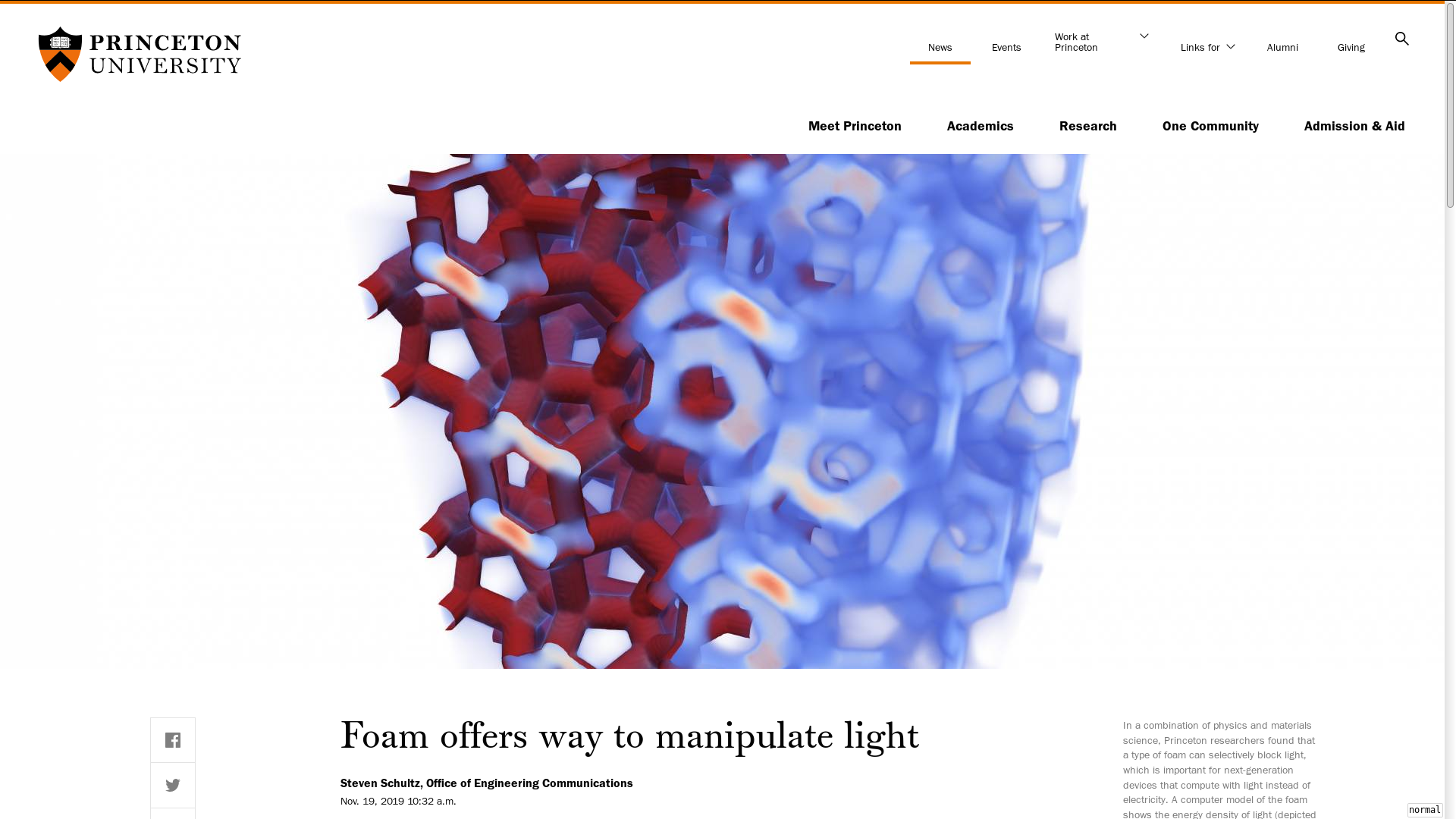
Can truly isotropic networks form a complete photonic band gap? A rigorous answer requires the photonic band gap to not only open up for finite approximants, but the gap has to remain open even in the thermodynamic limit.
To address this question numerically as accurately as currently possible, we designed a two-stage ensemble approach for a sequence of increasingly large photonic network structures. Comparing different types of short- and long-range order, we found that the apparent photonic band gaps of finite samples rapidly closed with an increasing system size — except for our sufficiently stealthy hyperuniform models, in agreement with the conjecture that stealthy hyperuniformity with sufficiently high chi values is a necessary condition for photonic band gaps to persist in isotropic disordered networks in the thermodynamic limit.